


 English
  русский
  Español
  Deutsch
  عربى
عربى -
A Rocker Switch is a compact and easy-to-operate manual control component. Its unique rocker-style actuation, combined with a toggle or momentary reset function, allows users to quickly switch circuit...View More >>
-
A micro switch is a small mechanical switch with a fast action mechanism, which is widely used in household appliances, industrial automation, automotive electronics, medical equipment, and other fiel...View More >>
-
Push button switches are widely used in various control systems with their diverse structural designs, high-strength material selection, and excellent performance. The products are available in a vari...View More >>
-
The internal structure of the piano key switch mostly adopts a mechanical or light-touch design. Some high-end models use capacitive sensing technology to achieve contactless operation, thereby improv...View More >>
-
The baby stroller gear switch is an innovative product independently developed by our company. We have applied for invention patents both domestically and internationally, which fully demonstrates the...View More >>
-
The knob switch adopts a high-sensitivity rotary contact structure, which has smooth operation and clear positioning, ensuring that every adjustment is accurate. The product has excellent durability a...View More >>
-
The KM trigger switch is a universal high-current switch designed for high-power power tools, with excellent current carrying capacity and stable performance. The internal fast-action structure ensure...View More >>
-
A door control switch, also known as a door magnetic switch or door status sensor, is a key electrical component widely used in industrial control, security systems, intelligent building automation, a...View More >>
-
The wiring harness is an overall wiring assembly that integrates multiple wires, cables, terminals, and connectors according to specific electrical design and mechanical structure requirements. It is ...View More >>
-
PCB control board is one of the indispensable core components in modern electronic devices. As the brain of the control system, it is widely used in many fields such as industrial automation, consumer...View More >>

Performance Introduction
Contact Us
PCB Control Board Manufacturers


PCB control board is one of the indispensable core components in modern electronic devices. As the brain of the control system, it is widely used in many fields such as industrial automation, consumer electronics, communication equipment, medical equipment, automotive electronics, new energy, etc. It not only provides physical support for electronic components, but also realizes electrical connection and signal transmission between components through preset conductive lines, and undertakes key functions such as data processing, power management, interface expansion, and real-time monitoring.
About SHQIJIA
Shanghai Qijia Electronics Co., Ltd. was founded in 2004. After more than two decades of development and accumulation, it has grown into a high-tech enterprise integrating the design, R&D, manufacturing, sales, and service of high-quality appliance switches, as PCB Control Board Manufacturers and PCB Control Board Factory in China, we establish a professional and reliable brand image in the industry.
The company's core product line, "shqijia," covers a wide range of AC and DC appliance switches, including micro switches, rocker switches, pushbutton switches, trigger switches, and rotary switches, as well as AC and DC circuit board modules and controllers. These products are widely used in AC and DC power tools, electric garden tools, cleaning equipment, household appliances, medical equipment (oxygen concentrators), generators, electric strollers, water pumps, and other electronic and mechanical fields, providing customers in various industries with highly adaptable core component solutions.
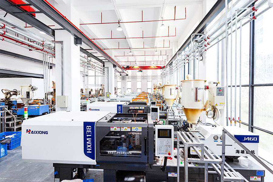
In 2025, the company opened a new factory Withover 20 assembly lines, more than 20 injection molding machines, and over 40 automated equipment, the company boasts an annual production capacity exceeding 80 million units, providing stable and efficient product supply support to customers worldwide. In addition, we support PCB Control Board Custom, the company possesses professional independent product and mold design capabilities, providing customized development services based on individual customer needs and precisely matching diverse application scenarios.
With superior quality, advanced manufacturing processes, competitive pricing, and comprehensive after-sales service, Qijia has earned widespread recognition and trust from customers worldwide.
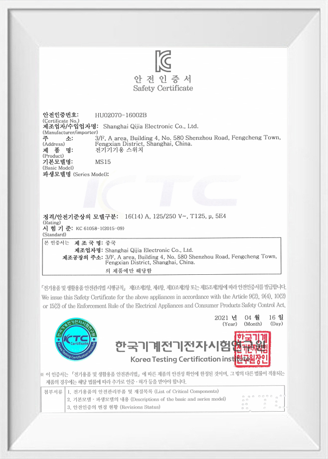
Certificate
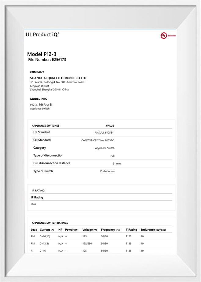
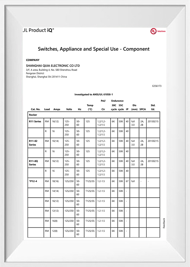
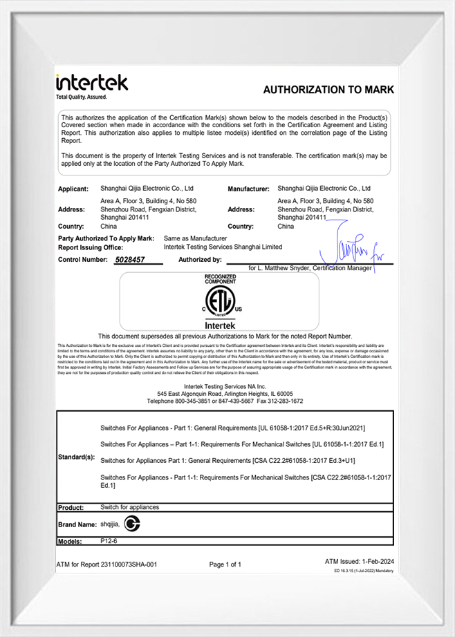
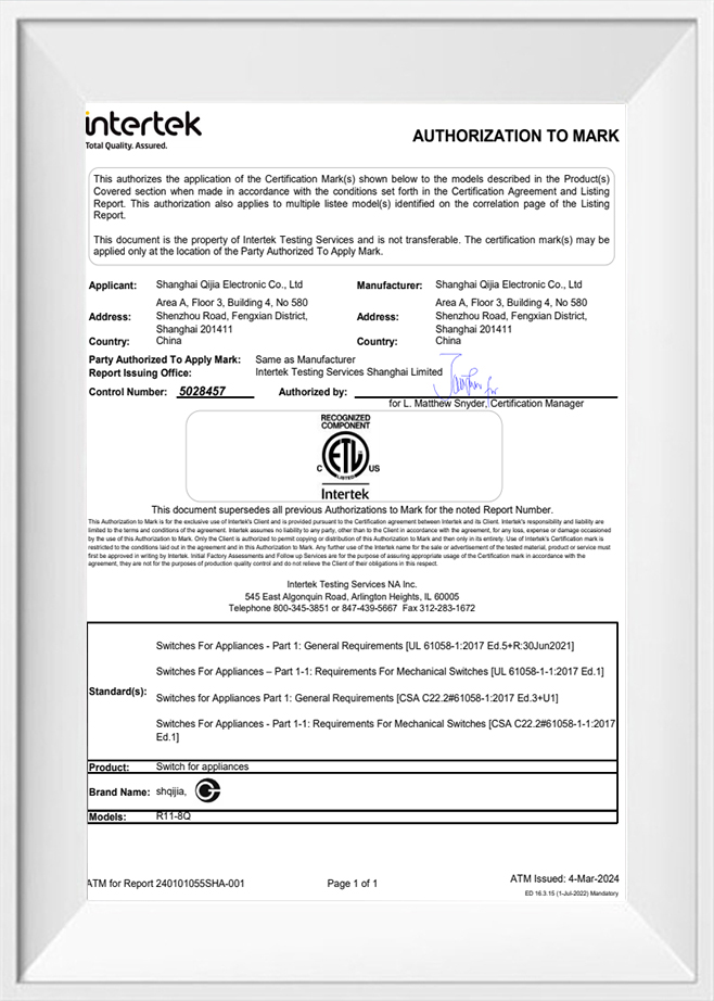
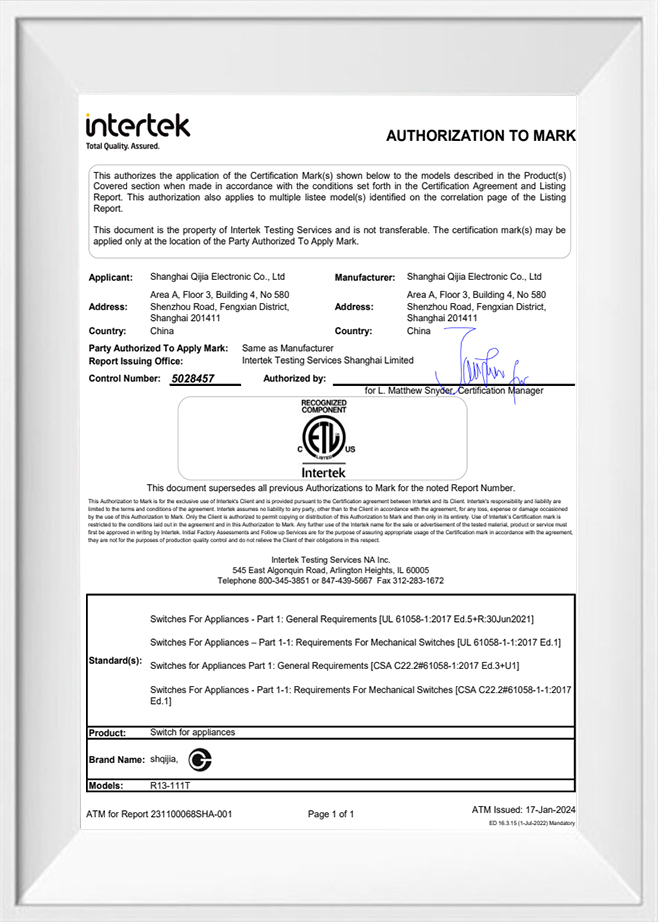
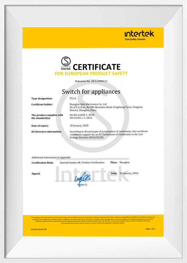
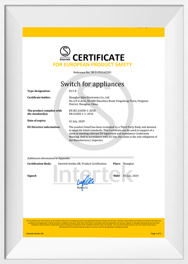
To ensure product quality and international compliance, the company has established a state-of-the-art switch testing center (laboratory) that is accredited by the US UL WTDP Witnessed Laboratory and fully ISO 9001 Quality Management System. Its entire product line has successfully passed multiple international certifications, including UL and ETL in the US, TÜV, CE, SEMKO, and CB in Europe, KC in South Korea, and CQC in China, fully meeting the access requirements of diverse global markets.
Latest Updates
Industry knowledge
High-Tech Control Solutions: Shanghai Qijia's Two Decades in Appliance Switches and PCB Modules
The PCB (Printed Circuit Board) control board, as the nerve center of an electronic system, has a value that far surpasses mere circuit connection. In modern electronics engineering, it represents the hardware realization platform for system functions, and is the key factor determining the level of product miniaturization, high performance, and intelligence.
I. The PCB Control Board Design Philosophy: Function, Density, and Constraints
Professional PCB control board design is a complex art of trade-offs, which must achieve the optimal balance among the following three core elements:
-
Functional Requirements: Ensuring that all circuit logic (such as microcontrollers, power management, sensor interfaces) operates according to design specifications.
-
Physical Density: Maximizing the integration of components and routing, while satisfying thermal management and manufacturing tolerances, to achieve miniaturization.
-
Constraint Management: Strictly adhering to Signal Integrity (SI), Power Integrity (PI), and Electromagnetic Compatibility (EMC) standards to ensure the system operates reliably in real-world environments.
A. High-Speed Signals and Integrity Challenges
For modern control boards operating at megahertz (MHz) or even gigahertz (GHz) frequencies, such as those used in data centers, 5G communications, or High-Performance Computing (HPC), the design focus has shifted from "connection" to "intact transmission."
-
Impedance Matching: Precisely controlling the characteristic impedance of transmission lines (traces), typically or (differential pairs), to eliminate signal reflections.
-
Crosstalk Control: Minimizing interference between adjacent signal lines by increasing the spacing between parallel traces, using Guard Traces, and optimizing the layer stack-up.
-
Power Plane Noise: Utilizing strategic placement of Decoupling Capacitors, combined with low-inductance power/ground planes, to supply stable transient current for high-frequency switching circuits and suppress Ground Bounce.
II. The Evolution of Integration and Manufacturing: The Driver of Miniaturization
As the demand for smaller electronic products becomes increasingly stringent, the technical development of PCB control boards is moving towards High-Density Interconnect (HDI) and System-in-Package (SiP).
-
HDI Technology: Achieves higher routing capacity per unit area by using laser drilling to create Microvias with diameters smaller than , and employing a Build-up process to add routing layers. This allows for successful routing beneath complex BGA (Ball Grid Array) packages.
-
Embedded Component Technology: Involves embedding passive components like resistors and capacitors directly into the internal layers of the PCB. This not only saves surface space but also shortens electrical connections, which is beneficial for improving high-frequency performance.
-
Component Conformality: Utilizing advanced packaging technologies such as Flip Chip and Wafer-Level Packaging (WLP) to create tighter and more efficient connections between the chip and the PCB.
III. Future Trends: Intelligence and Flexibility
The future of the PCB control board will be a platform that is more intelligent, flexible, and capable of adapting to harsh environments:
-
Flex and Rigid-Flex: These control boards can adapt to irregular internal spaces, enable 3D routing, and withstand a limited number of bends, making them the preferred choice for robotics, medical endoscopes, and wearable devices.
-
Integrated Sensing and Energy Harvesting: Future PCBs may not only carry circuits but also integrate printed sensors, and even printed batteries or energy harvesting units, becoming a self-sufficient intelligent module.
-
AI-Assisted Design (AI-Driven Layout): Utilizing artificial intelligence algorithms to optimize complex multi-layer board routing, especially in meeting Timing Constraints and thermal management requirements for hundreds of signals, which will significantly shorten the design cycle.
The PCB control board is the bridge connecting software algorithms to the physical world. Its professional design is no longer just about routing, but a holistic, systematic engineering approach that integrates electrical performance, thermodynamics, mechanical strength, manufacturing feasibility, and cost efficiency.
PCB Control Board Manufacturers that have been focusing on the development, production and sales of Switches for 21 years;
Products Links
Contact Information
Tel: +86-021-33752188
Phone: +86-15902103688
E-Mail: [email protected]
[email protected]
[email protected]Address: No. 580 Shenzhou Road, Fengxian District, Shanghai, China

